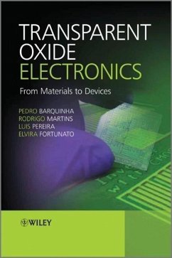
Transparent Oxide Electronics
From Materials to Devices
By Barquinha, Pedro; Martins, Rodrigo; Pereira, Luis; et al.
Transparent Oxide Electronics
From Materials to Devices
By Barquinha, Pedro; Martins, Rodrigo; Pereira, Luis; et al.
- Gebundenes Buch
- Merkliste
- Auf die Merkliste
- Bewerten Bewerten
- Teilen
- Produkt teilen
- Produkterinnerung
- Produkterinnerung
Transparent electronics is emerging as one of the most promising technologies for the next generation of electronic products, away from the traditional silicon technology. It is essential for touch display panels, solar cells, LEDs and antistatic coatings.
The book describes the concept of transparent electronics, passive and active oxide semiconductors, multicomponent dielectrics and their importance for a new era of novel electronic materials and products. This is followed by a short history of transistors, and how oxides have revolutionized this field. It concludes with a glance at…mehr
![Transparent Electronics Transparent Electronics]() Transparent Electronics250,99 €
Transparent Electronics250,99 €![Physical Properties of High-Temperature Superconductors Physical Properties of High-Temperature Superconductors]() Rainer WeschePhysical Properties of High-Temperature Superconductors229,99 €
Rainer WeschePhysical Properties of High-Temperature Superconductors229,99 €![Earth-Abundant Materials for Solar Cells Earth-Abundant Materials for Solar Cells]() Sadao AdachiEarth-Abundant Materials for Solar Cells176,99 €
Sadao AdachiEarth-Abundant Materials for Solar Cells176,99 €![Solar Cell Materials Solar Cell Materials]() Arthur WilloughbySolar Cell Materials183,99 €
Arthur WilloughbySolar Cell Materials183,99 €![Lithography Lithography]() Lithography195,99 €
Lithography195,99 €![Lead-Free Solders Lead-Free Solders]() Lead-Free Solders198,99 €
Lead-Free Solders198,99 €![Glancing Angle Deposition of Thin Films Glancing Angle Deposition of Thin Films]() Matthew M. HawkeyeGlancing Angle Deposition of Thin Films153,99 €
Matthew M. HawkeyeGlancing Angle Deposition of Thin Films153,99 €-
-
-
The book describes the concept of transparent electronics, passive and active oxide semiconductors, multicomponent dielectrics and their importance for a new era of novel electronic materials and products. This is followed by a short history of transistors, and how oxides have revolutionized this field. It concludes with a glance at low-cost, disposable and lightweight devices for the next generation of ergonomic and functional discrete devices. Chapters cover:
- Properties and applications of n-type oxide semiconductors
- P-type conductors and semiconductors, including copper oxide and tin monoxide
- Low-temperature processed dielectrics
- n and p-type thin film transistors (TFTs) - structure, physics and brief history
- Paper electronics - Paper transistors, paper memories and paper batteries
- Applications of oxide TFTs - transparent circuits, active matrices for displays and biosensors
Written by a team of renowned world experts, Transparent Oxide Electronics: From Materials to Devices gives an overview of the world of transparent electronics, and showcases groundbreaking work on paper transistors
- Produktdetails
- Verlag: Wiley & Sons
- 1. Auflage
- Seitenzahl: 320
- Erscheinungstermin: 9. April 2012
- Englisch
- Abmessung: 249mm x 170mm x 20mm
- Gewicht: 666g
- ISBN-13: 9780470683736
- ISBN-10: 0470683732
- Artikelnr.: 35046523
- Verlag: Wiley & Sons
- 1. Auflage
- Seitenzahl: 320
- Erscheinungstermin: 9. April 2012
- Englisch
- Abmessung: 249mm x 170mm x 20mm
- Gewicht: 666g
- ISBN-13: 9780470683736
- ISBN-10: 0470683732
- Artikelnr.: 35046523
Electronics: Fundamental Research or Heading Towards Commercial Products? 1
1.2 The Need for Transparent (Semi) Conductors 3 1.3 Reaching Full
Transparency: Dielectrics and Substrates 5 2 N-type Transparent
Semiconducting Oxides 9 2.1 Introduction: Binary and Multicomponent Oxides
9 2.1.1 Binary Compounds: the Examples of Zinc Oxide and Indium Oxide 9
2.1.2 Ternary and Quaternary Compounds: the Examples of Indium-Zinc Oxide
and Gallium-Indium-Zinc Oxide 12 2.2 Sputtered n-TSOs: Gallium-Indium-Zinc
Oxide System 16 2.2.1 Dependence of the Growth Rate on Oxygen Content in
the Ar+O2 Mixture and Target Composition 16 2.2.2 Structural and
Morphological Properties 18 2.2.3 Electrical Properties 22 2.2.3.1 Effect
of oxygen content in the Ar + O2 mixture 22 2.2.3.2 Effect of composition
(binary, ternary and quaternary compounds) 24 2.2.3.3 Effect of annealing
temperature 27 2.2.3.4 Additional considerations about the conduction
mechanisms in oxide semiconductors 30 2.2.3.5 Effect of thickness (ds) 39
2.2.3.6 Electrical stability measurements 39 2.2.4 Optical Properties 41
2.2.4.1 General considerations about the optical measurements 41 2.2.4.2
Effect of oxygen content in the Ar + O2 mixture 43 2.2.4.3 Effect of
composition (binary and multicomponent oxides) 44 2.2.4.4 Effect of
annealing temperature 46 2.3 Sputtered n-TSOs: Gallium-Zinc-Tin Oxide
System 49 2.4 Solution-processed n-TSOs 51 2.4.1 ZTO by Spray-pyrolysis 51
2.4.2 ZTO by Sol-gel Spin-coating 52 2.4.3 GIZO Sol-gel by Spin-coating 52
3 P-type Transparent Conductors and Semiconductors 63 3.1 Introduction 63
3.2 P-type Transparent Conductive Oxides 64 3.3 Thin Film Copper Oxide
Semiconductors 66 3.3.1 Role of Oxygen in the Structure, Electrical and
Optical Performance 70 3.3.1.1 Structure evaluation 70 3.3.1.2 Electrical
properties evaluation 71 3.3.1.3 Optical properties evaluation 74 3.4 Thin
Film Tin Oxide Semiconductors 75 3.4.1 Structure, Composition and
Morphology of Tin Oxide Films 79 3.4.1.1 Structure evaluation 79 3.4.1.2
Morphology evaluation 84 3.4.2 Electrical and Optical Properties of Tin
Oxide Films 84 3.4.2.1 Electrical properties evaluation 84 3.4.2.2
Capacitance measurements 89 3.4.2.3 Optical properties evaluation 92 4 Gate
Dielectrics in Oxide Electronics 101 4.1 Introduction 101 4.2 High-k
Dielectrics: Why Not? 102 4.3 Requirements 103 4.4 High-k Dielectrics
Deposition 106 4.5 Sputtered High-k Dielectrics in Oxide TFTs 106 4.6
Hafnium Oxide 107 4.6.1 Multicomponent Co-sputtered HfO2 Based Dielectrics
117 4.6.2 Multicomponent Dielectrics from Single Target 126 4.7 Tantalum
Oxide (Ta2O5) 130 4.7.1 Multicomponent Ta2O5 Based Dielectrics 133 4.8
Multilayer Dielectrics 138 4.9 High-k Dielectrics/Oxide Semiconductors
Interface 141 4.10 Summary 146 5 The (R)evolution of Thin-Film Transistors
(TFTs) 155 5.1 Introduction: Device Operation, History and Main
Semiconductor Technologies 155 5.1.1 Device Structure and Operation 155
5.1.2 Brief History of TFTs 161 5.1.3 Comparative Overview of Dominant TFT
Technologies 168 5.2 Fabrication and Characterization of Oxide TFTs 170
5.2.1 N-type GIZO TFTs by Physical Vapor Deposition 171 5.2.1.1 Effect of
oxygen content in the Ar + O2 mixture 172 5.2.1.2 Effect of composition
(binary, ternary and quaternary compounds) 173 5.2.1.3 Effect of annealing
temperature 179 5.2.1.4 Influence of source-drain electrodes material 181
5.2.1.5 Influence of passivation layer 185 5.2.2 N-type GZTO TFTs by
Physical Vapor Deposition 187 5.2.3 N-type Oxide TFTs by Solution
Processing 189 5.2.3.1 ZTO TFTs by spray-pyrolysis 189 5.2.3.2 ZTO TFTs by
sol-gel spin-coating 189 5.2.3.3 GIZO TFTs by sol-gel spin-coating 192
5.2.4 P-type Oxide TFTs by Physical Vapor Deposition 193 5.2.4.1 Cu2O TFTs
by sputtering 193 5.2.4.2 SnO TFTs by sputtering 195 5.2.5 N-type GIZO TFTs
with Sputtered Dielectrics 196 5.2.5.1 Tantalum-based dielectrics 198
5.2.5.2 Hafnium-based dielectrics 201 6 Electronics With and On Paper 211
6.1 Introduction 211 6.2 Paper in Electronics 212 6.3 Paper Properties 214
6.3.1 Structure, Morphology and Thermal Properties 214 6.3.2 Electrical
Properties of the Paper 218 6.3.2.1 The electrical resistivity 218 6.3.2.2
Electrical capacitance 219 6.3.2.3 Paper capacitance in less compact and
porous paper structures 220 6.4 Resistivity Behaviour of Transparent
Conductive Oxides Deposited on Paper 223 6.5 Paper Transistors 225 6.5.1
Current Transport in Paper Transistors 228 6.6 Floating Gate Non-volatile
Paper Memory Transistor 230 6.6.1 Memory Paper Device Feasibility and
Stability 233 6.6.2 Memory Selective and Charge Retention Time Behaviors
234 6.7 Complementary Metal Oxide Semiconductor Circuits With and On Paper
- Paper CMOS 237 6.7.1 Capacitance-Voltage and Current-Voltage
Characteristics of n/p-type Paper Transistors 240 6.7.2 N- and P-channel
Paper FET Operation 243 6.7.3 CMOS Inverter Working Principles 244 6.7.4
Paper CMOS Performance 246 6.8 Solid State Paper Batteries 249 6.9
Electrochromic Paper Transistors 252 6.10 Paper UV Light Sensors 255 7 A
Glance at Current and Upcoming Applications 267 7.1 Introduction: Emerging
Areas For (Non-)transparent Electronics Based On Oxide Semiconductors 267
7.2 Active Matrices for Displays 268 7.2.1 Display Market Overview and
Future Trends 268 7.2.2 Driving Schemes and TFT Requirements for LCD and
OLED Displays 269 7.2.3 Displays With Oxide-based Backplanes 271 7.3
Transparent Circuits 273 7.3.1 Inverters and Ring Oscillators 273 7.3.2 The
Introduction of Oxide CMOS 275 7.4 Oxide Semiconductor Heterojunctions 278
7.4.1 Oxide Semiconductor Heterojunctions In the Literature 278 7.4.2 GIZO
Heterojunctions Fabricated at CENIMAT 279 7.5 Field effect Biosensors 280
7.5.1 Device Types and Working Principles 280 7.5.2 Oxide-based Biosensors
Fabricated at CENIMAT 281 Index

