63,95 €
63,95 €
inkl. MwSt.
Sofort per Download lieferbar
payback
32 °P sammeln
63,95 €
63,95 €
inkl. MwSt.
Sofort per Download lieferbar

Alle Infos zum eBook verschenken
payback
32 °P sammeln
Als Download kaufen
63,95 €
inkl. MwSt.
Sofort per Download lieferbar
payback
32 °P sammeln
Jetzt verschenken
63,95 €
inkl. MwSt.
Sofort per Download lieferbar

Alle Infos zum eBook verschenken
payback
32 °P sammeln
  • Format: PDF

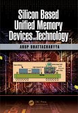
The primary focus of this book is on basic device concepts, memory cell design, and process technology integration. The first part provides in-depth coverage of conventional nonvolatile memory devices, stack structures from device physics, historical perspectives, and identifies limitations of conventional devices. The second part reviews advances made in reducing and/or eliminating existing limitations of NVM device parameters from the standpoint of device scalability, application extendibility, and reliability. The final part proposes multiple options of silicon based unified (nonvolatile)…mehr

Produktbeschreibung
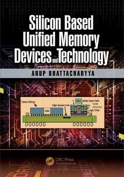
The primary focus of this book is on basic device concepts, memory cell design, and process technology integration. The first part provides in-depth coverage of conventional nonvolatile memory devices, stack structures from device physics, historical perspectives, and identifies limitations of conventional devices. The second part reviews advances made in reducing and/or eliminating existing limitations of NVM device parameters from the standpoint of device scalability, application extendibility, and reliability. The final part proposes multiple options of silicon based unified (nonvolatile) memory cell concepts and stack designs (SUMs). The book provides Industrial R&D personnel with the knowledge to drive the future memory technology with the established silicon FET-based establishments of their own. It explores application potentials of memory in areas such as robotics, avionics, health-industry, space vehicles, space sciences, bio-imaging, genetics etc.


Dieser Download kann aus rechtlichen Gründen nur mit Rechnungsadresse in A, B, BG, CY, CZ, D, DK, EW, E, FIN, F, GR, HR, H, IRL, I, LT, L, LR, M, NL, PL, P, R, S, SLO, SK ausgeliefert werden.

Autorenporträt
Dr. Arup Bhattacharyya has forty years of leadership and pioneering contributions in the area of microelectronics and nanoelectronics. He has contributed pioneering activities and innovations in process, device, interconnect, and integration of many generations of microelectronics and nano-electronics. His inventions include nearly 300 U.S. and international Patents and invention publications in technologies such as CCD, BIPOLAR, FET, NVM, FLASH, ANTIFUSE, SOI, BICMOS, SOLAR-CELLS, and SOC. Some of the applications of Dr. Bhattacharyya's inventions include electronic Memories, Microprocessors and Controllers, Random and Programmable Logic Devices, Nonvolatile Devices, Energy-conversion devices, ASICs, ASDs, and SMART Electronic Devices. He has experience in R&D leadership, Program management and Technology transfer, Technical Education and Consultancy, Strategic Planning, Infrastructure Development, Product Development, and Manufacturability. Additional experiences include University teaching, volunteering for science and engineering promotion, service to professional organizations, and consultancy to the UN.