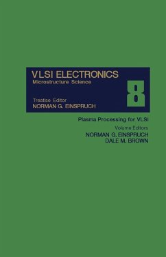
VLSI Electronics: Microstructure Science, Volume 8: Plasma Processing for VLSI (Very Large Scale Integration) discusses the utilization of plasmas for general semiconductor processing. It also includes expositions on advanced deposition of materials for metallization, lithographic methods that use plasmas as exposure sources and for multiple resist patterning, and device structures made possible by anisotropic etching.
This volume is divided into four sections. It begins with the history of plasma processing, a discussion of some of the early developments and trends for VLSI. The second section, Deposition, discusses deposition techniques for VLSI such as sputtering metals for metallization and contacts, plasma-enhanced chemical vapor deposition of metals and suicides, and plasma enhanced chemical vapor deposition of dielectrics. The part on Lithography presents the high-resolution trilayer resist system, pulsed x-ray sources for submicrometer x-ray lithography, and high-intensity deep-UV sources. The last part, Etching, provides methods in etching, like ion-beam etching using reactive gases, low-pressure reactive ion etching, and the uses of inert-gas ion milling. The theory and mechanisms of plasma etching are described and a number of new device structures made possible by anisotropic etching are enumerated as well.
Scientists, engineers, researchers, device designers, and systems architects will find the book useful.
Dieser Download kann aus rechtlichen Gründen nur mit Rechnungsadresse in A, B, BG, CY, CZ, D, DK, EW, E, FIN, F, GR, HR, H, IRL, I, LT, L, LR, M, NL, PL, P, R, S, SLO, SK ausgeliefert werden.

