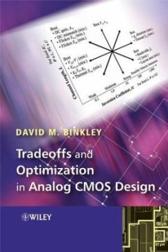
Analog CMOS integrated circuits are in widespread use for communications, entertainment, multimedia, biomedical, and many other applications that interface with the physical world. Although analog CMOS design is greatly complicated by the design choices of drain current, channel width, and channel length present for every MOS device in a circuit, these design choices afford significant opportunities for optimizing circuit performance.
This book addresses tradeoffs and optimization of device and circuit performance for selections of the drain current, inversion coefficient, and channel length, where channel width is implicitly considered. The inversion coefficient is used as a technology independent measure of MOS inversion that permits design freely in weak, moderate, and strong inversion.
This book details the significant performance tradeoffs available in analog CMOS design and guides the designer towards optimum design by describing:
An interpretation of MOS modeling for the analog designer, motivated by the EKV MOS model, using tabulated hand expressions and figures that give performance and tradeoffs for the design choices of drain current, inversion coefficient, and channel length; performance includes effective gate-source bias and drain-source saturation voltages, transconductance efficiency, transconductance distortion, normalized drain-source conductance, capacitances, gain and bandwidth measures, thermal and flicker noise, mismatch, and gate and drain leakage current
Measured data that validates the inclusion of important small-geometry effects like velocity saturation, vertical-field mobility reduction, drain-induced barrier lowering, and inversion-level increases in gate-referred, flicker noise voltage
In-depth treatment of moderate inversion, which offers low bias compliance voltages, high transconductance efficiency, and good immunity to velocity saturation effects for circuits designed in modern, low-voltage processes
Fabricated design examples that include operational transconductance amplifiers optimized for various tradeoffs in DC and AC performance, and micropower, low-noise preamplifiers optimized for minimum thermal and flicker noise
A design spreadsheet, available at the book web site, that facilitates rapid, optimum design of MOS devices and circuits
Tradeoffs and Optimization in Analog CMOS Design is the first book dedicated to this important topic. It will help practicing analog circuit designers and advanced students of electrical engineering build design intuition, rapidly optimize circuit performance during initial design, and minimize trial-and-error circuit simulations.

