70,99 €
inkl. MwSt.
Versandkostenfrei*
Versandfertig in 1-2 Wochen
payback
35 °P sammeln
  • Gebundenes Buch

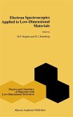
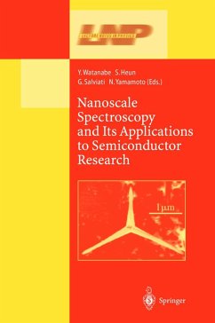
Fabrication technologies for nanostructured devices have be- en developed recently, and the electrical and optical properties of such nanostructures are a subject of advanced research. This book describes the different approaches to spectrosco- pic microscopy, i.e., Electron Beam Probe Spectroscopy, Spectroscopic Photoelectron Microscopy, and Scanning Probe Spectroscopy. It will be useful as a compact source of reference for the experienced reseracher, taking into account at the same time the needs of postgraduate students and nonspecialist researchers by using a tutorial approach throughout.

Produktbeschreibung
Fabrication technologies for nanostructured devices have be- en developed recently, and the electrical and optical properties of such nanostructures are a subject of advanced research. This book describes the different approaches to spectrosco- pic microscopy, i.e., Electron Beam Probe Spectroscopy, Spectroscopic Photoelectron Microscopy, and Scanning Probe Spectroscopy. It will be useful as a compact source of reference for the experienced reseracher, taking into account at the same time the needs of postgraduate students and nonspecialist researchers by using a tutorial approach throughout.
Autorenporträt
Yoshio Watanabe, NTT Basic Research Laboratories, Kanagawa, Japan / Stefan Heun, Sincrotrone Trieste, Italy / Giancarlo Salviati, Istituto MASPEC, Parma, Italy / Naoki Yamamoto, Tokyo Institute of Technology, Tokyo, Japan
Rezensionen
"This is an unusual collection and the vast audience of workers on semiconductor structure will want to have access to it." (Ultramicroscopy, 99, 2004)