74,99 €
inkl. MwSt.
Versandkostenfrei*
Versandfertig in 6-10 Tagen
payback
37 °P sammeln
  • Gebundenes Buch

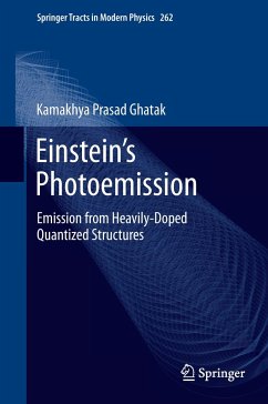
This monograph solely investigates the Einstein's Photoemission(EP) from Heavily Doped(HD) Quantized Structures on the basis of newly formulated electron dispersion laws. The materials considered are quantized structures of HD non-linear optical, III-V, II-VI, Ge, Te, Platinum Antimonide, stressed materials, GaP, Gallium Antimonide, II-V, Bismuth Telluride together with various types of HD superlattices and their Quantized counterparts respectively. The EP in HD opto-electronic materials and their nanostructures is studied in the presence of strong light waves and intense electric fields that…mehr

Produktbeschreibung
This monograph solely investigates the Einstein's Photoemission(EP) from Heavily Doped(HD) Quantized Structures on the basis of newly formulated electron dispersion laws. The materials considered are quantized structures of HD non-linear optical, III-V, II-VI, Ge, Te, Platinum Antimonide, stressed materials, GaP, Gallium Antimonide, II-V, Bismuth Telluride together with various types of HD superlattices and their Quantized counterparts respectively. The EP in HD opto-electronic materials and their nanostructures is studied in the presence of strong light waves and intense electric fields that control the studies of such quantum effect devices. The suggestions for the experimental determinations of different important physical quantities in HD 2D and 3D materials and the importance of measurement of band gap in HD optoelectronic materials under intense built-in electric field in nano devices and strong external photo excitation (for measuring physical properties in the presence ofintense light waves which alter the electron energy spectra) have also been discussed in this context. The influence quantizing magnetic field, on the EP of the different HD quantized structures (quantum wells, quantum well HD superlattices and nipi structures) under different physical conditions has been investigated. This monograph contains 100 open research problems which form the integral part of the text and are useful for both Ph.D aspirants and researchers in the fields of materials science, condensed matter physics, solid-state sciences, nano-science and technology and allied fields in addition to the graduate courses in modern semiconductor nanostructures offered in different Universities and Institutes.
Autorenporträt
Professor K. P. Ghatak is the First Recipient of the Degree of Doctor of Engineering of Jadavpur University in 1991 since the University inception in 1955 and in the same year he received the prestigious Indian National Science Academy award. He joined as Lecturer in the Institute of Radio Physics and Electronics of the University of Calcutta in 1983, Reader in the Department of Electronics and Telecommunication of Jadavpur University in 1987 and Professor in the Department of Electronic Science of the University of Calcutta in 1994 respectively. His present research interest is nanostructured science and technology. He is the principal co-author of more than 200 research papers on Semiconductor and Nanoscience in eminent peer-reviewed International Journals and more than 50 research papers in the Proceedings of the International Conferences held in USA and many of his papers are being cited many times. Professor Ghatak is the invited Speaker of SPIE, MRS, etc. and is the referee

of different eminent Journals.