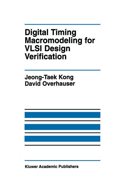
Digital Timing Macromodeling for VLSI Design Verification
-
- Hardcover
- Taschenbuch ausgewählt
-
Sprache:Englisch
146,99 €
inkl. gesetzl. MwSt.,
Beschreibung
Produktdetails
Einband
Taschenbuch
Erscheinungsdatum
03.10.2012
Abbildungen
XXI, 265 p.
Verlag
Springer UsSeitenzahl
265
Maße (L/B/H)
23,5/15,5/1,6 cm
Gewicht
446 g
Auflage
Softcover reprint of the original 1st edition 1995
Sprache
Englisch
ISBN
978-1-4613-5982-1
Digital Timing Macromodeling for VLSI Design Verification
first of all provides an extensive history of the development of simulation techniques. It presents detailed discussion of the various techniques implemented in circuit, timing, fast-timing, switch-level timing, switch-level, and gate-level simulation. It also discusses mixed-mode simulation and interconnection analysis methods. The review in Chapter 2 gives an understanding of the advantages and disadvantages of the many techniques applied in modern digital macromodels.
The book also presents a wide variety of techniques for performing nonlinear macromodeling of digital MOS subcircuits which address a large number of shortcomings in existing digital MOS macromodels. Specifically, the techniques address the device model detail, transistor coupling capacitance, effective channel length modulation, series transistor reduction, effective transconductance, input terminal dependence, gate parasitic capacitance, the body effect, the impact of parasitic RC-interconnects, and the effect of transmission gates. The techniques address major sources of errors in existing macromodeling techniques, which must be addressed if macromodeling is to be accepted in commercial CAD tools by chip designers. The techniques presented in Chapters 4-6 can be implemented in other macromodels, and are demonstrated using the macromodel presented in Chapter 3. The new techniques are validated over an extremely wide range of operating conditions: much wider than has been presented for previous macromodels, thus demonstrating the wide range of applicability of these techniques.
Noch keine Bewertungen vorhanden
Verfassen Sie die erste Bewertung zu diesem Artikel
Helfen Sie anderen Kundinnen und Kunden durch Ihre Meinung.
Kurze Frage zu unserer Seite
Vielen Dank für dein Feedback
Wir nutzen dein Feedback, um unsere Produktseiten zu verbessern. Bitte habe Verständnis, dass wir dir keine Rückmeldung geben können. Falls du Kontakt mit uns aufnehmen möchtest, kannst du dich aber gerne an unseren Kund*innenservice wenden.
zum Kundenservice