Silicon-on-Insulator Technology: Materials to VLSI Materials to VLSI
-
- Hardcover
- Taschenbuch ausgewählt
- eBook
-
Sprache:Englisch
146,99 €
inkl. gesetzl. MwSt.,
Beschreibung
Produktdetails
Einband
Taschenbuch
Erscheinungsdatum
03.10.2012
Abbildungen
XIII, 366 p.
Verlag
Springer UsSeitenzahl
366
Maße (L/B/H)
23,5/15,5/2,1 cm
Gewicht
581 g
Auflage
Third Edition 2004
Sprache
Englisch
ISBN
978-1-4613-4795-8
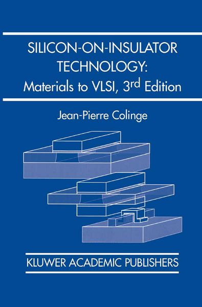
Silicon-on-Insulator Technology: Materials to VLSI, Third Edition
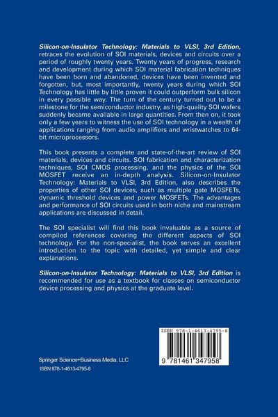
, retraces the evolution of SOI materials, devices and circuits over a period of roughly twenty years. Twenty years of progress, research and development during which SOI material fabrication techniques have been born and abandoned, devices have been invented and forgotten, but, most importantly, twenty years during which SOI Technology has little by little proven it could outperform bulk silicon in every possible way. The turn of the century turned out to be a milestone for the semiconductor industry, as high-quality SOI wafers suddenly became available in large quantities. From then on, it took only a few years to witness the use of SOI technology in a wealth of applications ranging from audio amplifiers and wristwatches to 64-bit microprocessors.
This book presents a complete and state-of-the-art review of SOI materials, devices and circuits. SOI fabrication and characterization techniques, SOI CMOS processing, and the physics of the SOI MOSFET receive an in-depth analysis.
Noch keine Bewertungen vorhanden
Verfassen Sie die erste Bewertung zu diesem Artikel
Helfen Sie anderen Kundinnen und Kunden durch Ihre Meinung.
Kurze Frage zu unserer Seite
Vielen Dank für dein Feedback
Wir nutzen dein Feedback, um unsere Produktseiten zu verbessern. Bitte habe Verständnis, dass wir dir keine Rückmeldung geben können. Falls du Kontakt mit uns aufnehmen möchtest, kannst du dich aber gerne an unseren Kund*innenservice wenden.
zum Kundenservice