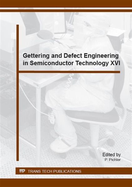
Gettering and Defect Engineering in Semiconductor Technology XVI (eBook, PDF)

PAYBACK Punkte
68 °P sammeln!
Collection of selected, peer reviewed papers from the GADEST 2015: Gettering and Defect Engineering in Semiconductor Technology, September 20-25, 2015, Bad Staffelstein, Germany. The 7 1 papers are grouped as follows: Chapter 1: Growth of Mono- and Multi-Crystalline Silicon; Chapter 2: Passivation and Defect Studies in Solar Cells; Chapter 3: Intrinsic Point Defects and Dislocations in Silicon; Chapter 4: Light Elements in Silicon-Based Materials; Chapter 5: Properties and Gettering of Transition Metals in Silicon; Chapter 6: Radiation- and Impurity-Related Defect Studies in Silicon and Germa...
Collection of selected, peer reviewed papers from the GADEST 2015: Gettering and Defect Engineering in Semiconductor Technology, September 20-25, 2015, Bad Staffelstein, Germany.
The 7 1 papers are grouped as follows: Chapter 1: Growth of Mono- and Multi-Crystalline Silicon; Chapter 2: Passivation and Defect Studies in Solar Cells; Chapter 3: Intrinsic Point Defects and Dislocations in Silicon; Chapter 4: Light Elements in Silicon-Based Materials; Chapter 5: Properties and Gettering of Transition Metals in Silicon; Chapter 6: Radiation- and Impurity-Related Defect Studies in Silicon and Germanium; Chapter 7: Thermal Properties of Semiconductors; Chapter 8: Luminescence and Optical Properties of Semiconductors; Chapter 9: Nano-Sized Layers and Structures; Chapter 10: Wide-Bandgap Semiconductors; Chapter 11: Advanced Methods and Tools for Investigation of Semiconductor Materials
The 7 1 papers are grouped as follows: Chapter 1: Growth of Mono- and Multi-Crystalline Silicon; Chapter 2: Passivation and Defect Studies in Solar Cells; Chapter 3: Intrinsic Point Defects and Dislocations in Silicon; Chapter 4: Light Elements in Silicon-Based Materials; Chapter 5: Properties and Gettering of Transition Metals in Silicon; Chapter 6: Radiation- and Impurity-Related Defect Studies in Silicon and Germanium; Chapter 7: Thermal Properties of Semiconductors; Chapter 8: Luminescence and Optical Properties of Semiconductors; Chapter 9: Nano-Sized Layers and Structures; Chapter 10: Wide-Bandgap Semiconductors; Chapter 11: Advanced Methods and Tools for Investigation of Semiconductor Materials
Dieser Download kann aus rechtlichen Gründen nur mit Rechnungsadresse in A, B, BG, CY, CZ, D, DK, EW, E, FIN, F, GR, HR, H, IRL, I, LT, L, LR, M, NL, PL, P, R, S, SLO, SK ausgeliefert werden.


