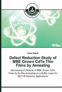
Defect Reduction Study of MBE Grown CdTe Thin Films by Annealing
Decreasing of Defects of MBE Grown CdTe F¿lms by Ex-Situ Annealing as a Buffer Layer for MCT IR Detector Applications
Versandkostenfrei!
Versandfertig in 6-10 Tagen
33,99 €
inkl. MwSt.

PAYBACK Punkte
17 °P sammeln!
MBE grown CdTe thin films were annealed in this study to decrease the number density of defects. For annealing, a system was designed and constructed. During anneals; anneal temperature, anneal time, anneal cycle and hydrogen gas effects were analyzed. The effects of annealing parameters were analyzed by SEM, AFM, Everson Etch method, resonance Raman spectroscopy, and Photoluminescence measurement. In our studies, dislocation density and Te precipitation decreased after annealing. Raman mode of CdTe at 144 cm-1 was investigated comprehensively and that mode was decided as Te E mode. Also, I2LO...
MBE grown CdTe thin films were annealed in this study to decrease the number density of defects. For annealing, a system was designed and constructed. During anneals; anneal temperature, anneal time, anneal cycle and hydrogen gas effects were analyzed. The effects of annealing parameters were analyzed by SEM, AFM, Everson Etch method, resonance Raman spectroscopy, and Photoluminescence measurement. In our studies, dislocation density and Te precipitation decreased after annealing. Raman mode of CdTe at 144 cm-1 was investigated comprehensively and that mode was decided as Te E mode. Also, I2LO/ILO ratio decreased with increasing annealing temperature and annealing time. I2LO/ILO ratio was approached to 1 at 80oK due to so-called 'resonance Raman scattering'. Extra peaks were also observed by Raman scattering.Surface roughness decreased with increasing cycle number.


