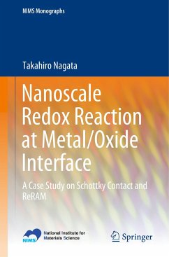
Oxide materials are good candidates for replacing Si devices, which are increasingly reaching their performance limits, since the former offer a range of unique properties, due to their composition, design and/or doping techniques.
The author introduces a means of selecting oxide materials according to their functions and explains metal/oxide interface physics. As he demonstrates, material development is the key to matching oxide materials to specific practical applications.
In this book, the investigation and intentional control of metal/oxide interface structure and electrical properties using data obtained with non-destructive methods such as x-ray photoelectron spectroscopy (XPS) and x-ray reflectometry (XRR) are discussed. Further, it shows how oxide materials can be used to support the development of future functional devices with high-k, ferroelectric, magnetic and optical properties. In closing, it explains optical sensors as an application of metal Schottky contact and metal/oxide resistive random access memory structure.

