Data Converters
-
- Hardcover ausgewählt
- Taschenbuch
- eBook
-
Sprache:Englisch
112,99 €
UVP
128,39 €
inkl. gesetzl. MwSt.,
Lieferung nach Hause
Beschreibung
Produktdetails
Einband
Gebundene Ausgabe
Erscheinungsdatum
22.02.2007
Verlag
Springer UsSeitenzahl
440
Maße (L/B/H)
24,1/16/3,3 cm
Gewicht
936 g
Auflage
2007
Sprache
Englisch
ISBN
978-0-387-32485-2
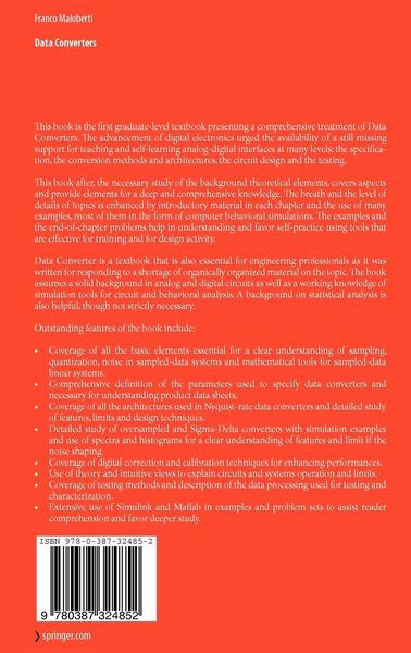
This book is the first graduate-level textbook presenting a comprehensive treatment of Data Converters. It provides comprehensive definition of the parameters used to specify data converters, and covers all the architectures used in Nyquist-rate data converters. The advancement of digital electronics urged the availability of a still missing support for teaching and self-learning analog-digital interfaces at many levels: the specification, the conversion methods and architectures, the circuit design and the testing. The book uses Simulink and Matlab extensively in examples and problem sets. This is a textbook that is also essential for engineering professionals as it was written in response to a shortage of organically organized material on the topic. The book assumes a solid background in analog and digital circuits as well as a working knowledge of simulation tools for circuit and behavioral analysis.
Kundinnen und Kunden meinen
Verfassen Sie die erste Bewertung zu diesem Artikel
Helfen Sie anderen Kund*innen durch Ihre Meinung
Kurze Frage zu unserer Seite
Vielen Dank für dein Feedback
Wir nutzen dein Feedback, um unsere Produktseiten zu verbessern. Bitte habe Verständnis, dass wir dir keine Rückmeldung geben können. Falls du Kontakt mit uns aufnehmen möchtest, kannst du dich aber gerne an unseren Kund*innenservice wenden.
zum Kundenservice